![]()
![]()
![]()
![]()
![]()
![]()
![]()
MARQUISE - An Embedded High Performance Computer Demonstration
Candy Culhane
National Security Agency
9800 Savage Rd
STE 6514
Ft Meade, MD 20755-6514
csculha@afterlife.ncsc.mil
Paul J. Boudreaux
The Laboratory for Physical Sciences
8050 Greenmeade Drive
College Park, MD 20740-4000
boudreau@glue.umd.edu
Ken Sienski
Red River Engineering
4204 Pike Court
Plano, TX 75093
sienski@idt.net
- Abstract:
- The goal of the MARQUISE project is to demonstrate the impact of advanced packaging technologies on a commercial high performance computer architecture. Multi Chip Modules (MCMs), diamond substrates, and phase change spray cooling are used together to shrink a 4 processor, 1 GByte memory version of the Cray J90 supercomputer from a cabinet system down to a form factor suitable for a 19 inch rack. Weight is reduced by 75% and volume is reduced by 80%. Code is currently executing on the MARQUISE test vehicle. The final SOLITAIRE prototype is scheduled for demonstration in late summer 1997.
- Keywords:
- CMOS, Diamond, Embedded, High Performance, J90, MCM, Miniaturization, Reliability, Spray Cooling, Thermal Management, Volume, Weight
Introduction
Current military processing requirements include real time processing, large data sets, and high data I/O throughput to keep up with the constant data flow from the sensor suites. The next generation of sensors will impose additional demands on I/O rates and will also drive increases in the processing performance required. The military currently requires a processing metric of 25 GFlops/ft3, and is driving towards 100 GFlops/ft3, with a future goal of 1 TFlop/ft3.
The traditional approach of designing custom hardware to ensure adequate performance has led to a wide variety of hardware with the additional burden of a large inventory of replacement parts. There is also a need for a pool of people with specialized knowledge that is very costly to maintain.
Economics are driving the military to decrease their dependence on custom hardware and highly specialized knowledge. There is a requirement for a common architecture. The processing algorithms must become software based. It is advantageous to write these algorithms in high level languages that are accessible to a wide population. Such a transition will enable the military to continually migrate to the newest hardware with minimal software impact and decreased dependence on a specialized knowledge base.
High Performance Computers (HPCs) can satisfy these processing requirements but traditionally they have been tethered to supercomputer installation sites. The machines are too heavy or too big, and some of them require extensive infrastructure support in the way of plumbing. It has not been possible to dramatically shrink the size of these HPCs because of the problems associated with heat extraction. A new packaging technology is required to simultaneously satisfy the demands of reduced weight and volume and provide self contained thermal management. Any strategy to embed commercial HPCs must also enable migration to the next generation of commercial machines.
The MARQUISE Project
The goal of MARQUISE is to demonstrate the impact of Advanced Packaging Techniques on Embedded High Performance Computers (HPCs). By integrating several packaging techniques now achieving maturity, MARQUISE combines high power, high performance commercial architectures with simplified thermal management techniques, while reducing weight and volume at the same time.
The packaging techniques chosen for MARQUISE are multichip modules (MCMs) for reduced equipment size, diamond substrates for improved circuit reliability, and spray cooling for highly efficient thermal management. These techniques have been mentored and developed under ARPA and NSA sponsorship since the early 1990s [1], [2].
The combination of these advanced packaging techniques gives rise to a new packaging paradigm that is technology independent and compatible with the constant improvement in commercially available general purpose CMOS HPCs. This enables a new capability to offer commercial supercomputers in an embedded form factor, suitable for military processing requirements.
The MARQUISE project began in late 1994. The initial phase of MARQUISE focused on two objectives: assessing the feasibility of replacing custom design high performance electronics with a general purpose HPC, and identifying a candidate HPC to use in the MARQUISE packaging demonstration.
An early task completed under MARQUISE was the study of the processing requirements for a wideband channelizer, a representative military problem. The processing required for the channelizer was divided into three stages: filtering, pulse detection, and parameter estimation. A first order analysis showed a sustained processing demand of 127 GFlops for filtering, 5.6 GFlops for pulse detection, and 41.7 MFlops for parameter estimation. This analysis indicated that it would remain more cost effective to use custom hardware for the first stage, and that the last stage was easily within the computation range of general purpose computers. The middle stage of pulse detection could be performed by a High Performance Computer. This study confirmed the basic premise that an embedded supercomputer could offer an alternative to custom military hardware.
The selection of a candidate HPC depended on several factors: a commercial design that was stable and current at the outset of the project so that planning would not be disrupted by product changes; a large enough product base such that a large quantity of die would be available for MCM process development work; a stable O/S and software compilers; and a company willing to work closely together with multiple team members and the Government.
The J90 High Performance Computer
The J90 was first announced by Cray Research Inc. in late 1994. The J90 was chosen for the MARQUISE project because it satisfied all of the criteria for a candidate HPC outlined in the previous section1.
The J90 is a Parallel Vector Processor (PVP) architecture with Uniform Memory Access (UMA). The flat memory architecture simplifies the programming model and reduces data migration. The compiler technology for this computer architecture is mature and efficient for many algorithms. The specifications for this machine are as shown:
 |
Architecture | PVP |
| Technology | CMOS | |
| Power required per 4 processor system | 550 Watts | |
| Cooling | Forced Air | |
| Clock Frequency | 100 MHz | |
| Processors per Module | 4 | |
| Memory per Module | 1 GByte DRAM | |
| Memory Bandwidth | 50 GBytes/sec | |
| Scalability | From 8 to 32 processors (2 to 8 modules) | |
| Peak scalar performance per processor | 100 MIPS | |
| Peak vector performance per processor | 200 MFlops | |
| I/O (per Y1 channel) | 50 MByte/sec |
Table 1 - J90 and Specifications
The J90 is built up from a fundamental building block (referred to as a System Element, or "SE") which can be broken down into two basic modules - the Processor Module and the Memory Module. The Processor Module contains four vector processors, an I/O element, and two Y1 channel interfaces.
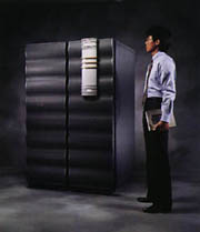
The Memory Module shown at right contains the network chips that interconnect the processors to the memory plus one Gbyte of DRAM and attendant memory bank controllers. This commercial module, including power converters mounted underneath the board and guiderails for insertion in the commercial cabinet, measures 19.5 x 20 inches and weighs 27 pounds.
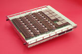
Figure 1 - A commercial J90 Memory Module
A System Element, which is one Processor Module combined with one Memory Module, constitutes the component to be miniaturized under the MARQUISE program. The two modules are repackaged onto one double-sided printed circuit board fully populated with MCMs. The board footprint is reduced from 16 x 19 inches to 9 x 10 inches.
Advanced Packaging Techniques
There are several challenges to miniaturizing a commercial HPC. A central requirement is to reduce weight and volume. In order to achieve the reduction in volume, something close to chip scale packaging is required to enable denser packaging of the microcircuits. MCMs were chosen as a way to achieve an approximate 4:1 volume reduction at the circuit board level. The decrease in physical packaging volume leads to a corresponding decrease in weight. Note that MCMs can also substantially improve the performance of an integrated chip set, but because full software and O/S compatibility with the commercial J90 was a requirement of this project, this advantage of MCMs was not included in this technology demonstration.
The increased power density of the MCM circuitry aggravates the thermal stress on the microcircuits. Diamond substrate was chosen as a method to evenly spread heat through the MCM to eliminate hot spots and improve microcircuit reliability. The additional weight and volume of the diamond material required is negligible.
Efficient heat transfer techniques are required to remove the same amount of heat from a greatly reduced volume. Spray cooling was chosen as a very efficient thermal management technique that adds little increase in weight, volume, and power consumption. In addition, spray cooling eliminates the need for heat sinks and their attendant weight and volume.
These packaging techniques are briefly described below; a fuller treatment is given in [3].
Multichip Modules
Most microelectronic circuits are packaged individually in what might be called Single Chip Modules (SCMs). A large amount of the surface area in an SCM is devoted to the package I/O. In some cases, such as large count Pin Grid Array (PGA) packages, the ratio of chip area to package area is 1:9. The commercial J90 uses an advanced packaging technique called Ball Grid Array (BGAs) which improves the ratio of chip area to total package area, but the ratio still falls far short of 1:1.
An MCM places several chips into one package. The use of thin film interconnect between the chips also improves the ratio between total chip area and package area. For example, under the MARQUISE program, a Processor Element (PE) MCM that incorporates the four chips required to implement one vector processor was designed. The resulting PE MCM occupies less area than the footprint for one of the four chips packaged in an SCM with the attached heat sink required for air cooling. This gives the desired 4:1 volume reduction in size.
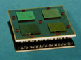
Figure 2 - One J90 vector processor repackaged as a 41 mm x 41 mm PE MCM
Four basic types of MCMs were developed under MARQUISE. These four types include a processor element (PE), a network element (NE), a memory element (ME), and an I/O element (IOE). The size of each MCM is 41mm x 41mm in order to optimize the design, manufacturing, and test process. The ME MCM design also incorporates stacked memory technology in the form of "mini" cubes.
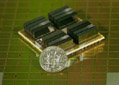
Figure 3 - 128 MBytes DRAM with memory bank controllers repackaged as an ME MCM
Diamond Substrate
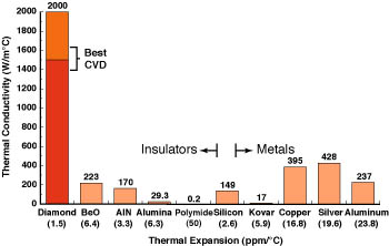
Manmade CVD synthetic diamond has three major characteristics that make it an ideal choice for use in MCMs - diamond is an electrical insulator [4], it has a coefficient of thermal expansion (1.5) close to that of silicon (2.6), and it has a high thermal conductivity (1500 W/mK). Of the materials commonly used as substrates, silver has the next highest thermal conductivity (428 W/mK), but silver is also an electrical conductor.
Figure 4 - Properties of materials commonly used in microelectronics packaging
One of the advantages of using diamond substrates for heat spreading is the improvement in reliability and subsequent increase in the mean time before failure of a microelectronic circuit. Many reliability problems of microelectronics stem from the overheating of silicon chips. Near room temperature, the relationship between the temperature of an integrated circuit and its expected operating lifetime predicts that every reduction of ten degrees Kelvin will double the mean time before failure of the device [5].
Experiments were conducted in 1991 to investigate the effect of diamond as a packaging material in single chip IC packages. An Integrated Circuit (IC) test vehicle was designed that incorporated resistive heaters and temperature sensing diodes. The ICs were packaged four ways: a ceramic Dual Inline Package (DIP), diamond coated DIP, ceramic Pin Grid Array (PGA), and PGA with diamond insert. Power ranging from 1 watt to 5 watts was applied to each IC resulting in a local hot spot under ambient room temperature conditions. Temperature measurements were recorded at eight locations, each of a varying distance from the hot spot. The most dramatic result was the measurement of a location 200 microns away from the same hot spot on the two PGA packages when five watts was applied. The temperature reading on the PGA with diamond insert was 80 degrees Centigrade less than the temperature reading taken at the same location on the control PGA [6]. Clearly, diamond had a dramatic effect in decreasing local heating.
The next step was to test diamond as a substrate material for MCMs. Experiments were performed in NSA labs in early 1995 using MCM test vehicles built on a rectangular alumina oxide and a round diamond substrate. Each substrate contained nine die which functioned as heaters. The die were patterned exactly the same on each MCM and the surface areas were comparable. A total of ten watts was supplied to each MCM.
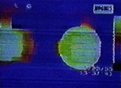 In still air conditions (passive cooling) with an ambient temperature of 24 degrees Centigrade, the experiment showed a temperature of 82 degrees Centigrade on the alumina and 55 degrees Centigrade on the diamond, for a delta of 27 degrees.
Figure 5 - False color thermal image of square ceramic and round diamond based MCMs operating in still air
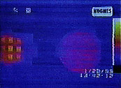 A second experiment was conducted with air flow (active cooling). This experiment showed a temperature of 45 degrees Centigrade on the alumina and 30 degrees Centigrade on the diamond, for a delta of 15 degrees. Note that the outlines of the chips are clearly evident on the ceramic substrate, while the diamond substrate appears isothermal.
Figure 6 - False color thermal image of square ceramic and round diamond based MCMs operating under forced air cooling
For a 15 degree delta, one would expect at least an improvement of approximately 3x in the mean time before failure of the circuit packaged with diamond versus one packaged with alumina.
A frequent objection to the use of synthetic diamond substrate is the cost. There are now several diamond merchants in the commercial marketplace and the price of diamond substrate has dropped dramatically. Shortly after the beginning of the MARQUISE program, a competitive bid was conducted for procurement of the diamond material. Two companies were selected to provide diamond material for MARQUISE - Diamonex and Norton Diamond Film. These manufacturers have been able to supply sufficient test pieces and finished product to permit full experimentation with innovative manufacturing methods of attaching diamond substrate to silicon based MCMs.
In the MARQUISE program, diamond substrate is attached directly to the silicon substrate of the ICs which provides a very efficient thermal path from the microcircuits to the diamond. The thickness of the material used to attach the diamond is less than a few microns, and does not introduce a significant thermal barrier. The thickness of the diamond substrate is 500 microns.
Spray Cooling
Spray cooling is used to remove the heat from the exposed surface of the diamond substrate. Spray cooling employs a phase change (from the liquid to gaseous state) to extract the heat from the surface it is sprayed against [7]. The phase change process is sustained by continuously coating the diamond with a uniform thin film of Flourinert. This Flourinert material is the same fluid used in the final process step for semiconductor and PWB manufacturing. Flourinert is used to clean contaminants from the components and is thus completely compatible with the finished computer electronics.
Spray cooling works by generating a fine mist of droplets which form a thin layer of fluid on the components to be cooled. The fluid begins to heat up once in contact with the radiant component. When the fluid reaches its boiling point, the molecules of liquid turn into a gas and "boil off" the component, thereby transferring the heat. The thin layer of fluid is replenished with a fine spray as the fluid evaporates. The surface temperature of the cooled electronics remains fairly constant, just below the boiling point of the flourinert (e.g., 56 degrees centigrade for FC-72).
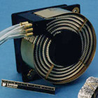
 The success of spray cooling is highly dependent on the precision of the formation of the droplets of fluid, which is very much like the fine mist sprayed from a perfume atomizer. The spray heads are micromachined nozzles that can be arranged to spray the electronics in an optimal fashion. Shown at right is a mockup of a spray head with fluid channels embedded in a clear plastic clamshell.
Figure 7 - A sample spray head arrangement positioned over an MCM
The flourinert vapor is exhausted from the clamshell enclosure and returned to an external condenser to complete the closed-loop system. A heat exchanger is used to condense the Flourinert and a standard 5 inch muffin fan blows across the condenser coils to exhaust the heat. Spray cooling imposes a very low power overhead, expending one watt for every twenty five watts extracted. 500 Watts of heat can be exhausted using a condenser coil packed into a five inch muffin fan.
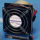
Figures 8 & 9 - Standard 5 inch muffin fan (Front and Back Views)
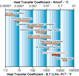 Spray Cooling is a very efficient technique for heat removal. The Heat Transfer Coefficient for spray cooling using Flourinerts approaches 5 W/cm2-degree Centigrade, which is an order of magnitude greater than jet impingement with flourinerts, two orders of magnitude greater than Air-Forced Convection, and three orders of magnitude greater than Air-Free Convection. The only methods more efficient are water based methods (Water-Boiling Convection and spray cooling using water) which cannot be employed when the circuits are exposed directly to the spray coolant.
Figure 10 - Heat Transfer co-efficients of various cooling technologies
Spray cooling also offers a wide margin of fault tolerance. If a pump fails, other pumps arranged in parallel can increase pumping capacity to prevent system shutdown. The failed pump can be replaced with snap in parts in a matter of minutes. The micromachined spray heads are arranged to provide overlapping coverage such that should a spray head become clogged, the remaining spray will still adequately coat the surface of the diamond. In fact, diamond is an ideal companion to spray cooling because diamond's superb thermal spreading characteristics ensure that even partial spray coverage of the diamond surface is sufficient to remove the heat from the entire MCM.
The packaging used for spray cooling is compact and self contained. It requires very small amounts of flourinert (amounting to tablespoons) and all fluids are recycled in a closed system environment. It is possible to package a system such that from an external point of view, it looks no different from an air cooled system. No auxiliary plumbing hookups are required. A final advantage of spray cooling is that it offers a thermal path that is independent of the mechanical path. This allows spray cooling to be used to "cocoon" COTS equipment for use in harsh military environments, without incurring the typical large costs (in terms of weight, volume, dollars, and time) of ruggedizing the electronic equipment.
Integration and Evaluation
The MARQUISE program required a substantial research and development investment, spanning three years. In order to manage the project, several milestones were defined, including
- Development of a diamond based die last MCM process
- Verification of the die last MCM process
- Optimization of atomizer placement for spray cooling
- Preliminary system test of the SOLITAIRE prototype
- Rack system integration
- Final SOLITAIRE system prototype demonstration
- Fluid compatibility studies
- Shock and Vibration testing
Many of these milestones are included in the two major program milestones, which are the demonstration of the lab test vehicle MARQUISE and the demonstration of the final prototype SOLITAIRE computer system.
Phase 1 Milestone - MARQUISE Lab Board Demo
This first major milestone required the construction of a lab test vehicle, also called MARQUISE. This board measures 16 x 19 inches, and contains four J90 vector processors and 512 MBytes of memory. The four vector processors and the I/O element are repackaged in MCMs. The network elements and memory subsystem use the standard commercial J90 packaging. This test board is air cooled.
The MARQUISE test vehicle was the driver for developing a diamond based die last MCM process. This test vehicle was also used to verify the die last MCM process and system net list translation from the J90 commercial product.
 The MARQUISE test vehicle completed assembly in Dec 1996 and was powered up for the first time in late Dec 1996. The board passed J90 scan testing in January 1997. During February 1997, the MARQUISE test board was mounted in a J90 test assembly and mated with the necessary life support equipment (such as power supplies and channel adapters) as well as diagnostic and test equipment.
Figure 11 - The MARQUISE lab board test vehicle, prior to heat sink attachment
Attempts to boot the UNICOS Operating System began in late February, which required some diagnostic trouble shooting due to very low level issues associated with scan chains of the hardware. Such issues are not unusual and are well understood. The O/S was successfully booted in mid April 1997 and by the next day MARQUISE had successfully compiled and executed 6 of the NSA benchmarks, exceeding all expectations of the performance of a lab test vehicle.
Phase 2 Milestone - SOLITAIRE System Prototype Demo
The second major milestone requires building the SOLITAIRE board, pairing the board with the spray cooling atomizers, enclosing the board in a hermetically sealed clamshell, mounting the clamshell in the Integration Platform, integrating all the peripheral electronics (including the clock board, Y1 channel adapter boards, the power converters, and a thermal fail safe monitoring system) and inserting the Integration Platform into a 19 inch rack along with all necessary "life support" systems including additional power converters, disk drives, and a front end laptop to serve as the operator console.
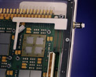
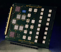
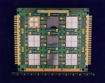 All of the MCM types are permanently attached to a double-sided printed circuit board to form the final prototype SOLITAIRE board. Four PE MCMs, four NE MCMs, and one IOE MCM mounted on the Logic Processing side, and eight ME MCMs are mounted on the Memory Module side. The 26 layer printed wiring board used is the same kind that is used in the Cray T902. The SOLITAIRE board netlist required 22 layers and implements 7800 nets. The routing of this design in 22 layers was a major program accomplishment.
Figure 12 - The SOLITAIRE prototype - Logic Processing View
All of the MCMs have Column Grid Arrays (CGAs) to accommodate the co-efficient of thermal expansion (CTE) mismatch between the MCM packages and the PWB. The height of the columns introduces sufficient "give" to handle this mismatch. The use of standard Ball Grid Arrays (BGAs) is not acceptable for a 41 mm x 41 mm MCM, and would suffer from component delamination from the board.
Currently, all of the logic MCMs have been manufactured and tested for correctness. The SOLITAIRE PCB has been manufactured and checked out 100% good against the design specification. Assembly of the ME MCMs has begun along with testing of the finished ME. A specialized tester was designed and fabricated to facilitate testing of the ME MCMs prior to being attached to the SOLITAIRE board.
Once the SOLITAIRE board is fully assembled and passes J90 acceptance testing, it will be inserted into an aluminum "clamshell" which provides a hermetically sealed environment for the electronics. This clamshell contains all of the spray cooling aerosol nozzles and embedded fluid channels to route the fluid to the nozzles. Studies were performed to determine the optimum configuration, number, and placement of the spray nozzles for each side of the SOLITAIRE board. Quick turn around Computer Aided Manufacturing (CAM) design tools and rapid prototyping enabled the thermal engineers to design, analyze, fabricate, test, and evaluate various configurations quickly and cheaply.
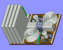 Next, the SOLITAIRE clamshell is mated with the system clock and channel adapter board and then mounted on an Integration Platform which also contains the spray cooler pumps, fans, condenser coils, fluid cartridge reservoirs. and a thermal warning and control (WAC) module. The thermal WAC was added to the system to prevent any damage to the SOLITAIRE board due to unforeseen thermal catastrophies. The Integration Platform is sized to fit within a standard 19 inch military rack.
Figure 13 - Concept drawing of 19 inch Integration Platform
The Integration Platform is designed to support up to four SOLITAIRE clamshells (for a peak processing capability of 3.2 GFlops), but the MARQUISE program will only demonstrate one SOLITAIRE board as a prototype proof of concept.
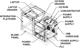 The Integration Platform will fit inside a standard military rack front panel height enclosure of 19.2 inches. The rack will also house multiple power converters, plus the VME card cage for the boot node running VXWorks, the SCSI card for the disks, the Y1 channel, and an ethernet card. The remaining pieces of the system, including a Sparc laptop (front end monitor), disks, and a concentrator, are also located in the rack.
Figure 14 - The Blue Rack configuration for an airborne SOLITAIRE system
The final evaluation of the system under this program is to execute standard NSA benchmarks and compare the results of the code running on the SOLITAIRE system with the results of the same code running on a commercial J90. The goal is to demonstrate that the SOLITAIRE system is binary compatible with the commercial J90 and gives the same performance.
Related Project Issues
The introduction of a new thermal management technique such as spray cooling raises several issues, especially if the prototype is to be subjected to operation in a hostile, non-computer room environment. Several system related spray cooling issues were identified during the research phase of the MARQUISE program, and included the effect of shock and vibration on the spray coolers and associated hardware, flourinert compatibility with standard microelectronic components, and any safety issues associated with catastrophic system failures.
Studies were designed to answer each of these questions. A test vehicle to spray cool a Sun microprocessor was designed to be subjected to shock and vibration experiments. Construction of this test vehicle is underway. Life testing of the pump motor components have been running for two years with no observed failures. Extensive fluid compatibility studies have been conducted on all components used in the SOLITIAIRE board as well as many standard microelectronic industry packaging materials. A few incompatible materials have been discovered and suitable substitute materials and components have been identified. Finally, a worst case analysis of catastrophic system failure involving power supply arcing causing flourinert to burn (at temperatures in excess of 400 degrees Centigrade) was conducted, leading to the conclusion that any resulting quantity of PFIB molecules created would be of insufficient volume to pose any toxic danger to humans.
Summary and Future Plans
The MARQUISE program establishes an advanced packaging road map to satisfy a requirement for embedded High Performance Computing. This packaging roadmap is enabled by the synergistic combination of MCMs, diamond substrate, and spray cooling. A program that proceeds from initial concept to evaluation has been described. These advanced packaging technologies are robust enough to support the miniaturization of an aggressive supercomputer with very high memory bandwidth and good overall machine balance.
It has been demonstrated that a complete Cray supercomputer can be miniaturized and still exhibit full software compatibility with the commercial product. A measured reduction of 75% in weight and 80% in volume has been achieved.
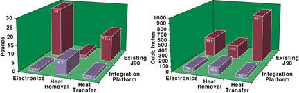
Figures 15 and 16 - System Size and Weight Reduction
This successful R&D program has spawned three new projects, which include:
Flight Demonstration
 One task is to demonstrate the SOLITAIRE system running military algorithms to perform functions currently computed using custom hardware. Planning has begun for the SOLITAIRE system to be integrated into a "Blue Rack" demonstration designated for experimental flight testing of new equipment on board the Air Force's Rivet Joint. [8]
Figure 17 - An RC-135 "Rivet Joint" aircraft taking off
This demonstration will allow for a direct connection to the current airborne sensor suite. The software would be supplied from a current project at Wright Labs that performs several military algorithms including deinterleaving and geolocation on ground based COTS computers such as the Cray EL and Silicon Graphics Indy, Indigo, and Power Challenge (This code is in the process of being ported to the Origin 200.)
One of the issues associated with an airborne demo is hooking into the available power supply. The power available on the Rivet Joint is from an airplane engine generator, which provides 200 Volts/400 Hz, three phase power. This power must be converted into two different formats, which are 110V/60Hz and 48 Volts DC (vdc). The 110V/60Hz power is used to power the standard peripheral equipment (disk drives, etc.) The 48 vdc is converted using the standard commercial J90 power converters to supply 5 vdc (for the memory devices) and 3.3 vdc (for the logic processors).
Embedded Scalable Node
A critical step on the tech transfer path is to identify an desirable embedded form factor and then apply just enough packaging technology in order to achieve that form factor while minimizing the cost and any attendant impact of the packaging on the computer to be miniaturized.
A new project has begun to foster this concept. A study is being performed to characterize the design space for what an embedded version of the SGI/Cray Research product Scalable Node would look like. Parameters such as weight, volume, memory configuration, technology risk, cooling technologies, and I/O configurations are all being evaluated against cost. Studies are being performed in conjunction with the Scalable Node product group during the commercial product design, instead of after-the-fact.
Miniaturized Power Converter
During the development of the MARQUISE program, it became apparent that a sizable amount of weight and volume in an overall computer system is budgeted for the power converters. This is also true in the Flight Demo for this project, where there are several stages of power conversion, as outlined above.
It also became apparent that significant weight savings could be achieved if power conversion could be performed directly on the board as close to the electronics as possible. If power conversion can be performed right next to the devices, then power can be transmitted to the electronics at high voltage, low current, which minimizes the amount and weight of copper required in the power bus bars typically required to distribute low voltage, high current power.
Some studies were performed under the MARQUISE program using stacked devices and spray cooling. The results of these studies [9], which demonstrated a spray cooled power converter with a density of 200 Watts/in3, are very promising. Future research in this area includes studying the use of both diamond material and spray cooling to achieve very dense, very efficient, miniaturized power converters.
Acknowledgement
The MARQUISE program is funded through NSA's participation in the High Performance Computing Systems (HPCS) portion of the High Performance Computing and Communications Initiative (HPCC).
The authors wish to acknowledge the many technical contributions of team members from Cray Research, Diamonex, Isothermal Systems Research (ISR), Norton Diamond Film, and Raytheon E-Systems.
Footnotes
1 The packaging is independent of the High Performance Computer chosen. For example, an MPP such as the T3E could be packaged in the same fashion. Any increase in the amount of heat dissipated by a different HPC can be easily handled by the diamond substrate and spray cooling.
2 In the Cray T90, two Gore High Speed printed wiring boards are laminated together to produce the number of layers required to support the memory bandwidth requirements of the Triton.