Michael Babst
Mike.Babst@dpslogic.com
Roderick Swiftrod.swift@dpslogic.com
Dave Strenskistren@cray.com
ABSTRACT:
This paper and presentation slides in PDF format.
DSPlogic has developed a hardware accelerated FFT algorithm for the FPGAs (Xilinx [1] Vertex-II Pro XC2VP50) attached to the Cray XD1 machine. In the paper we compare the results of the FFT running on the FPGA against running FFTW on the Opteron in terms of both accuracy and speed. We show that performance is highly dependent on the Opteron/FPGA communications architecture. A modular design structure was used to allow Opteron/FPGA communications to be isolated from the FFT algorithm itself. This architecture simplifies the processes of both changing the algorithm and adding new algorithms. It also allows FPGA/Opteron communications to be optimized and treated separately from the algorithm itself.
The paper starts with some background information about FFTW. Next we cover the motivation for pursuing an FFT algorithm on the FPGAs used on the Cray XD1 system and some background on that machine. The bulk of the paper then explains how the FFT was implemented on the Cray XD1 machine, with a description of the I/O architectural features. Since the number and format of the bits used in the FFT algorithm on the FPGA differ from those used on the Opteron, the next sections cover the issue of accuracy, and how to compare fixed point arithmetic against 32-bit IEEE floating point in terms of dynamic range and precision. Many combinations of precision are possible on the FPGA. The primary limitation of fixed-point arithmetic is dynamic range, which limits the maximum positive and maximum negative values of numbers used in the same computation. Many tradeoffs may be made among speed, FFT size, and precision. The speed is compared against the Opteron processors running FFTW.
The Fast Fourier Transform (FFT) was named one of the top ten algorithms of the 20th century, and continues to be a focus of current research. [2] They are used in many kinds of applications, most notably in the field of signal processing. A look at the FFTW web site [3] shows many of the different algorithms that can be used to calculate FFTs and how they compare to FFTW. Its performance is competitive even with vendor-optimized code, but unlike these programs, FFTW is not tuned to a fixed machine. Instead, FFTW uses a planner to adapt its algorithm to the hardware in order to maximize the performance. [4] Because of its performance, wide availability, and wealth of data at its web site, we choose it as the benchmark to which we compare our FPGA FFT design.
The Cray XD1 machine consists of a building block called a chassis. This chassis contains six node boards that each consist of; two Opteron processors, one Rapid Array Processor (RAP), an optional second RAP, and an optional Application Accelerator which consists of a Xilinx Vertex family FPGA and QDR SRAM. The six nodes are connected to a main board on the bottom of the chassis, which also contains a 24-port switch. Data from one Opteron is moved to the RAP via a Hyper Transport link and then through the switch to the receiving RAP and to the other Opteron.[5] [6]

The focus of our attention is on the node board as seen above. Note that the FPGA is directly attached to the second RAP using a Hyper Transport type link. This gives the machine a very low latency between the Opteron and the FPGA, about 0.3 microseconds, and a bandwidth of 1.6 GB/s in each direction. We show later in the paper the importance of this 1.6 GB/s bandwidth because it becomes the limiting performance factor in the FFT design on the FPGA.
For an example of another application running on the Cray XD1 machine using the Application Accelerator, refer to the paper from Los Alamos National Laboratory [7] showing a speedup of 34.4x on their traffic simulation application. Another interesting paper showing an application's boost in performance via FPGA, though not on the Cray XD1, is by the University of Southern California [8] showing a performance of 26.6 GFlops on a 32-bit matrix multiply routine.
In order to provide a design that is easy to upgrade, optimize, and customize, a modular design approach was used. Our tests indicate, as we will show, that performance is entirely limited by the Opteron/FPGA communications. Therefore the I/O interface is a very important part of the design and will also be discussed.
The modular design of the application and the division between the Opteron and the FPGA is shown in the next figure. The application consists of four primary layers, the Cray API, I/O Management, the FFT library, and the end-user software application.
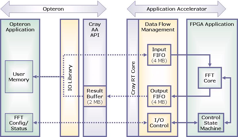
The Cray API (blue boxes) provides the low-level interface between the Opteron and the FPGA. [5] It consists of both FPGA cores and a library of function calls that are supplied from Cray. On the Opteron side, the Cray Application Accelerator software API provides functions such as loading, unloading, and resetting the FPGA. It also provides a simple method of writing data to and from the FPGA. On the FPGA side, the Rapid-Array Transport (RT) Core provides the low level communications interface to the Cray XD1 fabric. A QDR SRAM interface core is also provided to communicate with the SRAM attached to the FPGA.
The I/O management layer (yellow boxes) provides a greatly simplified,
framed, streaming data interface between the FFT software and hardware
layers. It provides simple software function calls such as
loadframe() and getresult() to send and receive
programmable length blocks of data, called frames, to and from the FPGA
application, the FFT design in this case. The Data Flow Management FPGA
core manages all communications with the host processor and the RT core.
It also provides input and output FIFOs to decouple the FPGA and Opteron
processing. Refer to Appendix 1 for the syntax of the API.
The FFT Library (green boxes) consists of an FFT core and a software API.
The software API consists of a single function, fft_init(),
which sets the FFT length and direction (forward/inverse). The FFT FPGA
core has been created using a combination of off-the-shelf cores and custom
VHDL programming to optimize for the XD1. The FFT core utilizes a Radix-2
decimation-in-frequency algorithm and is capable of continuous throughput
at 1 complex sample per clock cycle, with a maximum clock frequency of
200 MHz.
The end-user software application (also in green boxes) utilizes both
the FFT Library API and the I/O Management API. The user's data starts in
the Opteron's memory, organized as complex samples, each sample requiring a
64-bit format, described later. A simple function,
dspio_init() is called first to load the bitstream into the
FPGA and performs the initialization. Next, dspio_config()
is called to set the frame length used for communications with the FPGA.
A communications frame of data may consist of one or more FFT blocks.
The user then calls fft_init() to set the FFT length and
direction.
Input data is then sent to the core using the loadframe() function.
The user provides a pointer to the base address of the input data. The
loadframe() function may be called repeatedly until all
input data is transferred to the core. If the input FIFO is temporarily
full, the loadframe() function will return immediately with
a notification code.
FFT results data is retrieved from the core using the getresult()
function. Again, the user provides a pointer to where the FFT results
should be written. If the result is ready, one communications frame of
FFT data will be copied to user memory. If the result is not ready,
getresult() will return immediately with a notification
code. The getresult() function may be called repeatedly until
all FFT results are returned.
The purpose of this section is to describe the user data formats and the data flow between the Opteron and the FPGA.
The format for FFT input and output data is shown in the following figure.
The FFT length, N, may be between 32 and 65536.
In order to use pipelining to minimize the effects of
communications latency, it is useful to process multiple FFTs at once.
Therefore the entire input dataset length will consist of M
complex samples. The example provided here will compute non-overlapping
FFTs of this data.
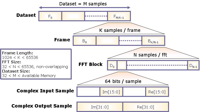
The data set must first be divided into M/K communication
frames, each containing K samples. Each frame may contain
one or more FFT blocks, each with N complex samples. The
I/O Management FPGA Core requires the frame length to be between
1024 and 65536. For example, N = 65536 must use one FFT per
frame, N = 1024 may use between one and 64 FFTs per frame,
and N = 32 must use between 32 and 2048 FFTs per frame.
The architecture is designed to provide the fastest possible FFT performance and maximum FFT throughput (in FFTs per second). However, it is clearly very inefficient if a single 32-bit FFT is to be computed.
The figure also shows that each complex input and output sample is represented by a 64-bit word, with the lower 32 bits reserved for the real part and upper 32 bits for the imaginary part. The input data utilizes 16-bit fixed point format and the output uses 32-bit fixed point format to allow bit growth for accurate computation at each stage of the FFT. More details on the precision of the FFT computations are discussed below.
Data pipelining is required to achieve maximum FFT performance. Multiple frames of input data may be sent to the FPGA before the first FFT result is returned. The time from the first input transmission to the first output result is the FFT latency. A diagram of this processing pipeline is shown in the following figure.

When the user calls loadframe(), data is sent to the input
FIFO on the FPGA. This forward transfer time is limited by the Cray XD1
fabric to:

where Fclk is the FPGA clock frequency. This corresponds to a maximum forward data transfer rate of

or 1.6 GB/s for Fclk = 200 MHz.
The FFT core is capable of processing data continuously at one sample per FPGA clock. The processing delay of the FFT core is approximately 1.5 FFT blocks, or:

The data is then transferred to the output FIFO at a rate of 1.6 GB/s. The FFT result is then transferred by the FPGA to a "result buffer" in Opteron memory, without CPU interaction. This transfer requires 9 clock cycles to transfer 8 64-bit words. This return frame transfer time is also limited by the Cray XD1 fabric to:

This corresponds to a maximum return data transfer rate of

or 1.42 GB/s for Fclk = 200 MHz.
Finally, the data is copied from the result buffer in Opteron memory to the user memory area on the Opteron. Experiments have shown that this transfer time is variable based on the Cray XD1 system performance, buffer memory locations and data types. However, typical performance in the current implementation is approximately 1.1 GB/s. Therefore the time to copy data from the result buffer to the user memory area is approximately

The total latency to the first FFT result is therefore

After simplification we have

The current implementation of the FFT uses fixed point computations. Fixed point numbers may be viewed as floating point numbers without the exponent and with a variable mantissa width. The lack of an exponent limits the dynamic range (largest and smallest number that may be represented. The exponent may be selected ahead of time, but must be common to all numbers. The exponent (or scaling) may also change during computations in a known, fixed manner. Therefore the resulting exponent may often be different than the input exponent but nonetheless applies to all output numbers.
The example shown here starts with a 16-bit fixed point input and allows precision (bit) growth throughout each stage of the computation. The result is a 32-bit output. The bit growth allows computations to be performed and the output to be represented without scaling/rounding effects. Other variations are possible, such as 24-bit input and 24-bit output. However scaling and rounding are required at each stage of the FFT computation in order to fit the result in the 24-bit output. This is similar to what happens in floating-point computations. [9]
The 16-bit input and 32-bit output was selected primarily for the convenience of not having to worry about scaling. It is important to note that the 16-bit fixed point arithmetic performed in the FPGA is not the same as doing 16-bit fixed point arithmetic on the Opteron. On a typical microprocessor with a fixed precision function unit, like a 32-bit floating point add unit, at every calculation there is a rounding error. So a 16-bit fixed point add unit would have two 16-bit input numbers and one 16-bit output number. On the FPGA the functional units are not all the same size (i.e. precision). Since the FFT algorithm is a 16 stage calculation and at each step an addition bit is used, such that for the FFT calculation two 16-bit fixed point numbers are the input, but one 32-bit fixed point number is the output. All 32 bits are preserved and sent back to the Opteron.
When comparing the precision of the results between the Opteron and the FPGA, we also need to look at how the precision is stored in an 32-bit IEEE floating point number. Recall that for single precision floating point numbers, 1 bit is used for the sign, 8 bits are used for the exponent, and 23 bits are used for the mantissa. So when comparing the 32-bit floating point with the 16-bit fixed point, the 7-bit difference in numerical format accounts for a significant portion of the accuracy capability.
A very simple measure of the precision of a fixed point number in terms of decimal notation is:
      16-bit accuracy = 1/(216) is on the order of 10-5
      23-bit accuracy = 1/(223) is on the order of 10-7
However, the accuracy of the FFT result depends on many more factors, such as the type of rounding/truncation (if any) used after each computation stage and the accuracy of the "twiddle factors" used in the computation. The bit growth to 32-bits at the output allows the precision to be maintained throughout the computation, even to a higher level of precision that is possible with 32-bit floating point numbers. An improved method of measuring the accuracy of the FFT is to used a normalized metric, such as the method described on the FFTW website [3]. The error between a high-precision FFT algorithm and the FPGA output is computed as

where the L2 norm is defined as
 .
.Using this methodology, the actual L2 norm accuracy of the 16-bit in/32-bit out FPGA FFT is measured between 2.0e-5 and 3.5e-5. This is commensurate with results for other single-precision FFT algorithms described on the FFTW website, as shown in the next figure. Finally recall that using 16-bit input/32-bit output was primarily for convenience. Other tradeoffs between speed, accuracy, and FFT size may also be made. In the future as more FPGA real estate becomes available, we should be able to fully implement a 64-bit floating point algorithm.

This section describes the expected speed performance of the FFT design on the FPGA. As with the accuracy section, getting a pure one-to-one comparison is difficult. The first thing to realize, from the Opteron side, is that when the Opteron is doing an FFT calculation, the function units are busy and can not work on anything else. When the FPGA works on the FFT, the Opteron may have spare processing bandwidth for other calculations. As the FPGA sends its results back, it uses separate circuitry to send the data to the Opteron's memory, so the Opteron's function units are available.
The other major difference between measuring the Opteron's performance and the FPGA performance is latency. Since everything is measured from the perspective of the Opteron's memory, the results from the FPGA have a latency associated with them, since they must traverse the Hyper Transport link to and from the FPGA. Therefore running single short FFTs will not perform well on the FPGA.
The FPGA is capable of processing 1 complex sample (represented by 64 bits) at every clock. The maximum clock speed is 200 MHz for a maximum processing bandwidth of 1.6 GB/s. The actual clock speed for the 16/32-bit test design is 175 MHz, with a maximum processing bandwidth of 1.4 GB/s. As shown above the maximum rate at which the FPGA can return data to the Opteron is limited to 1.4 GB/s due to the extra clock cycle required every 8 64-bit word transfers. Therefore, the theoretical maximum processing rate is limited by the fabric to 1.4 GB/s, or 175 complex samples/second.
A second limitation on the processing bandwidth is that there is
currently a 2 MB limit on the size of the Opteron memory space that
the FPGA can write to. Therefore the getresult() function
must continuously copy data from this buffer to the end user data buffer.
Experiments have shown that these general memory-to-memory transfers
average approximately 1.1 GB/s, depending on buffer memory locations
and data types. However special care when aligning buffers and selecting
data types can improve this figure. Nonetheless, the memory-to-memory
transfer rate is a second limit on the performance.
Finally, a third limitation exists when the loadframe() and
getresult() functions are used because the Opteron must be
time-shared to send the data to the FPGA and also to copy data from the
result buffer to the user data buffer. This reduces the I/O processing
bandwidth by an additional factor of 2. This is a significant impact on
performance and slows processing bandwidth to approximatley
(1.1)/2 = 550 MB/s. This is a "worst case" performance that will
be used as a lower bound on the expected performance of the FPGA-based FFT.
Further optimizations have improve performance beyond this rate. This rate will
also be improved further when the size limitation on the result buffer is removed.
Cray indicates that this will occur in one of the next releases.
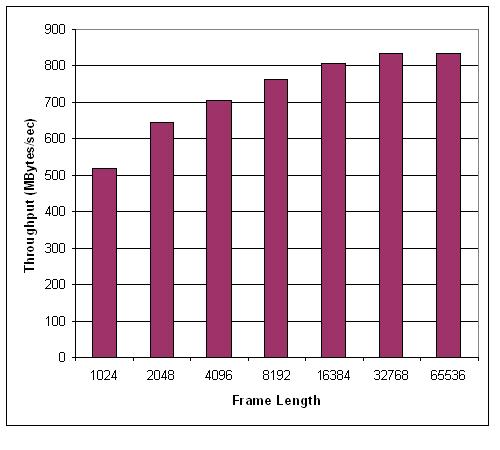
These three processing rates; 1.4 GB/s, 1.1 GB/s, and 550 MB/s each correspond to an FFT computation time based on the number of complex samples in the FFT. Again, the 1.4 GB/s represents the theoretical maximum, 550 MBps represents the absolute worst case, and 1.1 GB/s represents a reasonably achievable number after optimizations have been made. These expected results are shown in the following figure. The figure also shows the published performance of the FFTW algorithm [3] running on a Model 246 Opteron for comparison purposes. It can be seen that a processing rate of 1.4 GB/s or 1.1 GB/s will always outperform the Opteron based FFT. However the FPGA underperforms the Opteron for the worst case 550 MB/s at small FFT sizes. The current state of optimizations demonstrate a sustained throughput of over 800 MB/s.

The next graph shows the expected latency of the FFT, based on the pipeline description provided earlier. This represents the time needed to get the first FFT result frame back. This also demonstrates the need to run a large amount of data through the FPGA to overcome this latency.

The following table shows the actual measured results prior to optimization.
The FFT size and frame length were varied while the total number of samples
was maintained constant. The TX columns represent the average time duration or
throughput for the loadframe() operation. The RX colums
represent the average time duration or throughput for the getresult()
functions.
The table shows that the loadframe() throughput is optimal
at larger frame sizes while the RX getresult() throughput
remains relatively constant at about 1.1 GB/s. Therefore for best
performance, it is recommended that smaller FFT sizes be grouped into
larger frames for transmission to the FFT, provided that a low latency
is not required.
	 Frame   Number    FFTs/    Total
FFT size  Size   of Frm   Frames  Processed   Avg Duration(us)      Throughput(MB/s)
   N       K        F       K/N     Nproc   Total   TX     Rx     Total    TX      RX
 65536   65536      8        1     524288   932.6  403.0  526.0   562.2  1301.0   996.7
 32768   32768     16        1     524288   462.5  205.9  255.1   566.8  1273.3  1027.8
 16384   16384     32        1     524288   231.3  106.3  123.9   566.6  1233.3  1058.1
  8192    8192     64        1     524288   116.9   56.0   60.3   560.8  1169.3  1086.6
  4096    4096    128        1     524288    60.4   30.0   29.7   542.1  1090.8  1101.7
  2048    2048    256        1     524288    32.8   18.0   14.5   499.4   912.2  1129.6
  1024    1024    512        1     524288    19.2   11.1    7.9   426.0   739.0  1037.2
   512    1024    512        2     524288     9.3    5.4    3.7   441.8   753,5  1098.7
   256    1024    512        4     524288     4.6    2.7    1.8   443.7   745.5  1130.2
   128    1024    512        8     524288     2.3    1.4    0.9   442.9   744.7  1126.5
    64    1024    512       16     524288     1.2    0.7    0.5   441.0   741.0  1117.9
    32    1024    512       32     524288     0.6    0.3    0.2   441.4   742.0  1127.8
A combined throughputs of approximately 560 is achieved
without any optimization. In order to optimize the results further, a new function,
txrx() was created to manage the processing of the entire dataset for
the end user. This function accepts a pointer to the input dataset and writes the
result to another pointer location provided by the user. The function does not
return until all samples in the dataset are processed. Using this optimized method,
we have measured total throughputs in excess of 800 MB/s, an improvement of approximately
50% over the separate loadframe() and getresult()
function calls. Nonetheless, not all applications are as I/O intensive as the
FFT and, for example, might have a much smaller amount of output data than input
data. Therefore, the loadframe() and getresult() functions
may still remain convenient for other applications.
Finally, the following figure shows the expected speedup ratio of processing time for the Opteron based FFTW divided by the FPGA-based FPGA processing time for I/O rates of 1.4 GB/s (theoretical maximum), 1.1 GB/s (expected future performance), and 800 MB/s (current actual sustained throughput). As can be seen, the processing improvement is greatest for larger FFT sizes. The performance improvements for a two-dimensional FFT are expected to be even greater.
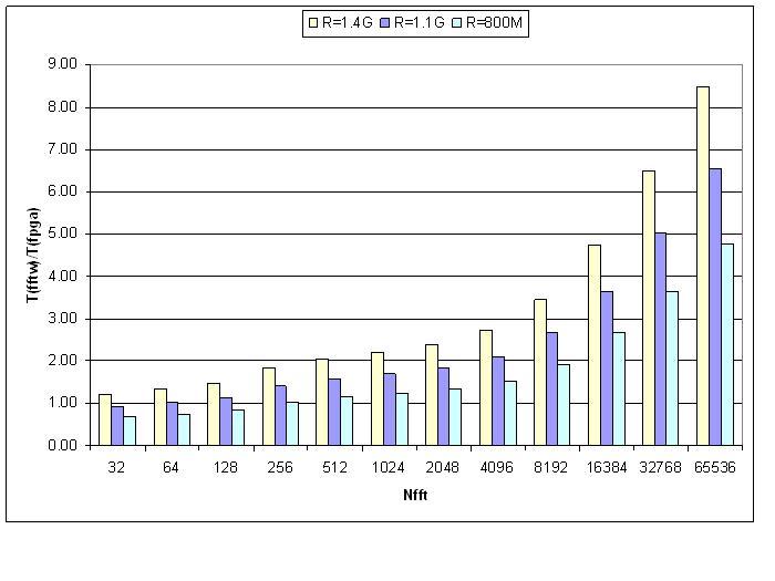
We have shown that using the FPGAs attached to the Cray XD1 to calculate one dimensional FFTs is feasible and currently yields at least a 4.75 times speedup for a FFT size of 65536, with a potential of up to 8.5 times. We have also demonstrated using 16-bit input/32-bit output fixed point data provides accuracy that is comparable to many single-precision algorithms, but not as accurate as the best single-precision algorithms. It can also can be moved to a higher level of precision with the caveat that constraints of the Virtex II Pro-50 might lower the speed or the maximum FFT size. The Virtex-4 will allow even greater FFT sizes, processing rates, and precision. We have also demonstrated that the performance is limited by the I/O interface to and from the FPGA. As I/O optimizations are improved, performance of the FFT will also improve. Finally, we described a modular design will ease the effort of porting other algorithms to the FPGAs attached to the Cray XD1.
The DSPlogic I/O Library API interface:
      FPGA Initialization
          int32 dspio_init( char fpgafile[], int32 verbose );

      I/O Configuration
          int32 dspio_config(
                uint32  nq_frm_in,    input frame length (64-bit words)
		uint32  nq_frm_out,  output frame length (64-bit words)
                int32   verbose );

      Close FPGA
          int32 dspio_close ( int32 verbose );

      Send data to FPGA
          int32 dspio_loadframe (
                const uint64 *datap,     pointer to input data
                uint32 frame_param       frame parameters
                int32  verbose );

      Read data from FPGA
          int32 dspio_getresult (
                uint64  *datap,           pointer for result data
                int32 verbose );

      I/O Status
          fpga_struct dspio_status ()
                uint64 app_id;        application ID
                uint32 comp_status;    comp status
                uint32 nfrm_received;    number of frames received by FPGA
                uint32 nfrm_returned;    number of frames returned by FPGA
                uint32 inbuf_depth_qw;   input buffer depth
                uint32 outbuf_depth_qw;   output buffer depth
                uint32 max_inbuf_depth_qw;  maximum input buffer depth
                uint32 max_outbuf_depth_qw;  maximum output buffer depth
                uint64 err;                   error code

      Control registers
          int32 dspio_appcfg (
                uint32  regid,           control register ID (0-7)
                uint64  val );

      Status registers
          uint dspio_appstat (
                uint32  regid,          status register ID (0-7)
                int32 verbose );
1 All jobs run on the Cray XD1 pacific.cray.com.